Up to 10% of electronic waste is made up of printed circuit boards, which are the basic building blocks for most electronic devices. A glass fibre reinforced epoxy resin is used to produce the insulating substrate, which contains additional, relatively toxic substances that act as flame retardants. However, it is a virtually non-recyclable material, so only metals can usually be reused from a discarded circuit board.
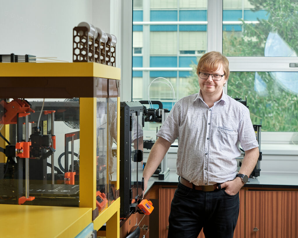
"Our goal is not only to eliminate materials that cannot be recycled during production but to develop and test a whole alternative electronics manufacturing process that is more environmentally friendly. Polymeric substances that are used in 3D printing, such as PET, among others, can be used to produce the substrate. After their appropriate modification to meet electronic product requirements, these will be used to replace epoxy resin," described Dr. Petr Veselý from the Department of Electrotechnology at the Faculty of Electrical Engineering of the Czech Technical University in Prague.
In addition to the 3DP Lab - Development and Research of Materials for 3D Printing in Electronics group, headed by Dr. Veselý, the research is also being carried out by staff from the Department of Polymers at the University of Chemistry and Technology in Prague, led by Dr. Čadek. "Our task is precisely the development and production of 3D printing strings that will have suitable properties for the production of carrier substrates. At the same time, these will be used after the end of their service life as raw material for the re-production of the printing string," comments Jonáš Uřičář, a student involved in the project.
3D printing will simplify production technology
In the conventional method of manufacturing printed circuit boards, a copper layer is chemically etched to form conductive motifs for interconnecting individual components. These are then connected to the circuit board, usually by soldering. However, this method of production is energy intensive and uses potentially hazardous substances and significant amounts of water.
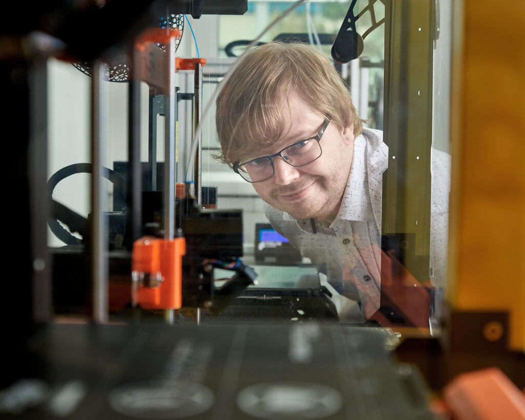
Using 3D printing technology, it is possible to produce printed circuit boards with electronic components already encapsulated in the substrate body, which are interconnected during subsequent printing with electrically conductive ink. Encapsulation ensures the mechanical integrity of the circuit, which would otherwise be reduced compared to conventional solutions due to the inferior mechanical properties of recycled plastics. This alternative manufacturing process eliminates energy- and chemical-intensive processes, and thus can contribute significantly to reducing the carbon footprint of electronic product manufacturing, according to Dr. Veselý.
"In addition to the environmental aspect, the incorporation of 3D printing technology also brings the possibility of a flexible response to any changes in product design and greatly simplifies the production process. This makes it ideal, for example, for the production of prototypes or smaller production series, where a significant reduction in production costs can be expected," added Dr. Veselý. However, the research also aims to move the development of this solution towards large-scale production and wider use in industrial practice. 3D printing technology can be replaced for large production runs by injection moulding using the same input material in the form of recycled thermoplastic.
So far, researchers from FEE CTU and UCT are testing the technology on single-layer printed circuit boards. Initial results were presented at the International Spring Seminar on Electronics Technology conference in Temesvár, Romania, in May 2023. However, as multi-layer boards (typically 4 to 16 layers) are required for most modern electronics circuits, the research group's efforts in this area will continue. Together, they are submitting a project proposal to the Czech Technology Agency's Environment for Life programme call, which, if awarded, should provide funding for further successful development of the presented solution.
1. Source TheRoundUp.org.